The high-speed photodiode circuit in Figure 1 uses a low capacitance PIN photodiode (PD), load resistance (RL), and a high-speed operational amplifier (U).
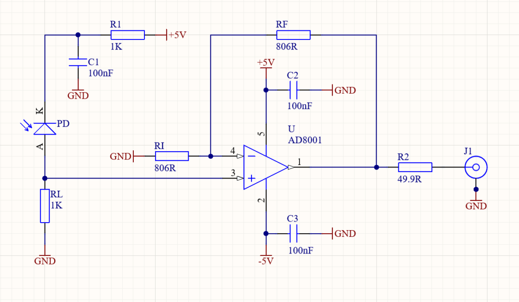
In this configuration, the photodiode is reverse biased and used in photoconductive mode. The short circuit current from the photodiode is forced to pass through the resistor RL. This current flowing through the RL resistor results in a voltage drop across it. The operational amplifier in non-inverting mode amplifies the voltage across the RL resistor. The output voltage of the amplifiers depends on feedback resistors RF and RI.
The components used in the circuit are given as an example and should be chosen based on your application. The output voltage for this circuit can be calculated using equation 1.

It is important to take attention when connecting components and routing printed circuit board (PCB). The photodiode leads should be as short as possible. Furthermore, traces between components should be as short and thick as feasible. By abiding by these guidelines, parasitic capacitance and inductance between component connections on the PCB will be reduced. It is important to take into account the current return path, hence using a solid ground plane is advised to reduce the circuit loop’s inductance. Bypass capacitor should be placed as close as possible to the supply pin of the operational amplifier.