Often, when designing printed circuit boards (PCBs), people do not even think about the materials used for their production. Unfortunately, these materials are critical to the performance of PCBs. That’s why I decided to talk about what you need to think about when choosing PCB materials. This article will be useful for both the novice and the experienced designer. I think so because we will go over the basic parameters of PCB materials and how they affect the performance of the manufactured PCB.
PCB stackup
First of all, before we start talking about PCB materials, we need to remember what a PCB stackup consists of. A PCB stackup refers to the arrangement of core, prepreg, and copper foil that make up a PCB.
Prepreg
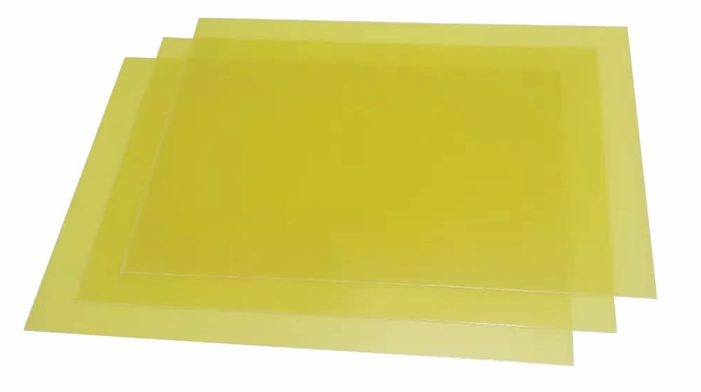
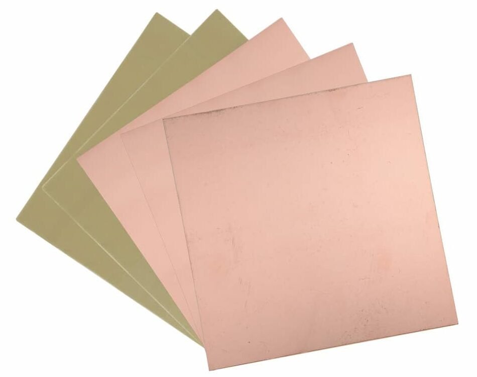
Prepreg is a sheet of the board reinforcement material which has been pre-impregnated with a synthetic resin such as epoxy. It is partially cured and often called the B-stage. All that sounds complicated, but prepreg is just a fiber weave/cloth that is impregnated with resin bonding agent. Prepreg is binding material and it either binds two cores or a core and a copper foil. You can see what prepreg looks like in Figure 1.
Core
Core similarly to prepreg is a sheet of the board reinforcement material impregnated with a synthetic resin such as epoxy but this time it is fully cured. This fully cured sheet is often called the C-stage. The core is rigid compared to the prepreg. Most often, the core, this rigid base material, is laminated with copper on one or two sides. These are commonly referred to as Copper Clad laminate (CCL). An example of the core is shown in Figure 2.
Copper foil
Copper foil is a thin sheet of copper metal used to fabricate the conductive traces in PCBs. Copper is the most commonly used metal foil for PCB manufacturing. It comes in many different thicknesses. The most common copper thicknesses are 17um (1/2oz) and 35um (1oz). As you can see in Figure 3, it is somewhat similar to baking foil.

4-layer PCB stackups
In the production of multilayer PCB, alternating prepreg layers and cores (CCL) materials are laminated together, at high temperature and pressure using a hydraulic press. The heat melts the prepreg and the pressure helps to bond all the layers together. When the formation cools, we have a laminate that is further processed in a similar way to a double-sided core.
Now let’s examine one of the most common 4-layer PCB stackups. This stackup is shown in Figure 4 and Figure 5.


In order to produce this 4-layer PCB with a finished thickness of 1.6mm, the manufacturer would start with a copper clad FR4 core material that is 0.71mm thick and has 35um (1oz) copper foil on both sides. After the core is processed through inner layer imaging, the prepreg of 0.37mm thickness and outer copper layers of 17um (1/2oz) would be added. As I mentioned, the prepreg is called “B stage” fiberglass. It is not rigid until heat and pressure are applied to it. Thus, allowing it to flow and bond the copper layers together as it cures. When the stackup is ready, it is then placed between two thick steel plates and placed into the lamination press. After cooling, the material is ready to move on to the next process. Finally, after via metallization, the outer copper layers are also metallized, and their thickness increases to approximately 35um (1oz).
The entire fabrication example for this board was described based on a stackup offered by one manufacturer. A 4-layer stackup may vary from manufacturer to manufacturer. For example, manufacturer may use two layers of prepreg, one after the other, to achieve the desired thickness.
I should also mention that the time, temperature, and pressure of the press cycle vary between manufacturers. For example, 170 Tg FR4 is heated to 190 °C, pressed at 300 PSI for 150 minutes.
Key properties of dielectric materials
There are many different material properties that can be measured in a laminate. However, we can highlight a few of the most important ones in circuit design. These properties are:
Glass transition temperature (Tg)
The glass transition temperature is a phenomenon of amorphous polymers. At this temperature, polymers undergo a transition from being a hard and relatively-brittle condition to being in a viscous or rubbery state. Tg is an important feature of polymer behavior. It marks a region of dramatic changes where the laminate deviates from its
existing linear state (CTE) and expands at a much higher rate. When the temperature of the material exceeds Tg, the laminate expands at a rate greater than below Tg. I know that it is somewhat difficult to understand, so I drew a picture for visualization, which is shown in Figure 6. The expansion is greatest on the Z axis. For FR4 material, the typical Tg temperature is 130°C.

Decomposition temperature (Td)
The decomposition temperature is the temperature at which a PCB material chemically decomposes. Once a material exceeds this temperature, changes to its properties are irreversible. For FR4 material, the Td temperature is somewhere around 350°C. This is important at the moment of PCB assembly, when the components are soldered onto the board. Most solder temperatures during PCB assembly are in the 200 ºC to 250 ºC range. So when choosing materials for your PCB, keep in mind that Td should be higher than the melting point of your solder.
Thermal Expansion (CTE)
The coefficient of thermal expansion is the rate of expansion of a PCB material as it heats up. CTE is measured in parts per million (ppm) expanded for every degree Celsius that it is heated. CTE impact on the X-Y axis is controlled primarily by the reinforcement (woven glass). As a result, along the X and Y axes, the CTE is generally low, around 15 ppm per degree Celsius. The CTE in the X-Y direction does not change much even as the material’s temperature increases above Tg.
The expansion in the Z-axis is usually at a rate significantly larger than in the X-Y axis, especially at temperatures above Tg. This expansion is determined by the resin system.
So why am I explaining all this to you? What does it have to do with PCB design? Well, to the designer, expansion is a concern from two perspectives: warpage of the assembly and damage to the plated through holes.
The difference in CTE between the package/lead and board is directly related to stress in the solder. The most common form of solder joint fatigue is caused by thermal cycles, which, because of mismatches in the CTE between the part and the board, induce strain in the solder joint.
And speaking of plated through holes, now we know that the z-axis resin expands without restriction of the glass fibers. This expansion has enough force that, with a large number of thermal cycles, the pressure exerted by the expanding resin will crack and rip the thin copper via plating apart, creating a stress crack leading to intermittent or an electrical open through the via.
Thermal conductivity (K)
Thermal conductivity is the property of a material to conduct heat. Low thermal conductivity means low heat transfer, while high conductivity means high heat transfer. The measure of the rate of heat transfer is expressed in watts per meter-kelvin (W/mK).
The conduction of heat through a material is directly proportional to the thermal conductivity constant of the material, the cross-sectional area of the conductive path, and the temperature difference across the material conducting the heat.
Most PCB substrates have a thermal conductivity of around 0.4 W/mK. This is quite low compared to copper, whose k is around 360 W/mK. Therefore, more heat will be carried away by copper plane layers in a PCB than by the dielectric material.
Dielectric Constant (Er or Dk)
Dielectric constant, also called permittivity or relative permittivity (Er), is the ratio of the capacitance of electrodes with a specific material as the dielectric between them to the capacitance of that same configuration with a vacuum or air as the dielectric.
The dielectric constant is a function of the resin and the glass or other reinforcement ratio, so the prepreg styles should be chosen carefully. Every base material has its own Dk, based in large part on the ratio of reinforcement glass to epoxy resin. Even the same material from different manufacturers may have a different Dk. Standard FR-4 has a dielectric constant of 3.9 to 4.8 (at 1MHz).
The dielectric constant varies with frequency and generally decreases as frequency increases. At high frequencies, electric power loss increases. This is one reason why materials with low dielectric constant values are preferred for high frequency applications. Substrates suitable for high-frequency applications are those whose dielectric constant remains relatively the same over a wide frequency range.
Dissipation Factor (Df)
The dissipation factor is also known as the loss tangent or dielectric losses. In any case, these losses are the absorption of electromagnetic energy by the board material in a varying electric field. So it is caused by a PCB’s internal prepreg and core layers. The extent of dielectric loss depends on the properties of the dielectric material, such as its dissipation factor and dielectric constant.
A lower dissipation factor indicates lower energy loss and is desirable for high-frequency applications where signal integrity is critical. A lower dissipation factor improves signal integrity, and there is less signal loss at high frequencies. It is important to consider the dissipation factor when designing PCBs for high-frequency applications, as excessive energy loss can lead to signal degradation and reduced performance.
The dissipation factor of FR4 typically ranges from 0.015 to 0.025, depending on the specific grade and composition.
Summary
In this blog post, we discussed basic PCB materials and how they affect the performance of the PCB. We also looked at a standard 4-layer PCB stackup. Here, we only scratched the surface of the PCB materials. I highly recommend you read more about this topic, because when designing complex PCBs, knowing the parameters of these materials is extremely important.