Welcome back to the second part of this series on building a DIY alarm system circuit. In the previous article, I explored the various components that make up this robust security solution, including the LTE module, USB-C charging circuit, SIM card, rechargeable Li-ion batteries, microcontroller, and siren. These components work together to provide a comprehensive alarm system that can be customized and built according to each individual’s specific needs.
In this article, I will delve into the crucial aspects of designing the printed circuit board (PCB) layout and routing. The PCB is a fundamental component of any electronic device, serving as the platform for connecting and arranging all the individual components into a cohesive circuit. A well-designed PCB layout ensures optimal performance, signal integrity, and ease of assembly.
By the time you finish reading this article, you’ll have a clear idea of how to design a PCB layout that not only works great but also makes sure all the components fit together smoothly. So let’s get started and discover the crucial steps and techniques that will guarantee that our alarm PCB will work flawlessly.
If you didn’t catch the first part of this series, I strongly suggest giving it a read. It’ll give you a good grasp of the components we’re using in our DIY alarm system circuit.
Layer stackup
I opted for a 4-layer Printed Circuit Board (PCB). Why? Well, there were a few key factors that influenced my choice. Firstly, I wanted to keep the PCB as compact as possible, considering the space constraints of my project. By utilizing a 4-layer PCB, I had more room to route traces and strategically place components, ensuring better signal integrity and minimizing noise interference.
Additionally, the use of a 4-layer PCB offered improved power and ground plane distribution, which is vital for maintaining stability and reducing signal crosstalk or electromagnetic interference. This is particularly important for a PCB with RF components.
In order to ensure the lowest PCB production cost, I chose the standard layer stackup offered by the manufacturer. This stackup is shown in Figure 1.

Board layout
Board layout, also known as PCB (Printed Circuit Board) design, involves the physical arrangement of components and routing of traces on a board. It starts with importing the netlist, which contains information about the connections between components from the schematic design software to the PCB design tool.
My preferred approach to board layout involves initially grouping components into smaller blocks that I can layout individually. I find that this method enhances my understanding of spacing and overall layout. By breaking down the design into these smaller blocks, I can focus on each section separately, leading to a more convenient layout procedure. This systematic methodology enables me to progressively integrate these smaller sections, resulting in a more accessible and efficient board layout as a whole.
Now, let’s delve into the placement and routing of the individual components within the electrical circuit.
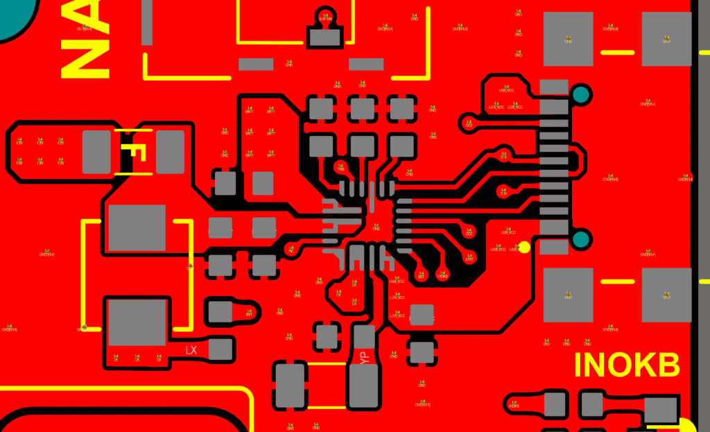
Piezo driver layout
Before proceeding with the layout of the DRV2700 circuit components, it is crucial to consider three primary factors:
- Ensuring a large ground (GND) plane to provide good thermal dissipation.
- Incorporating a large boost (BST) plane to minimize resistance and inductance in the traces.
- Placing both feedback resistors in close proximity to the FB pin to reduce coupling from the SW pin.
Now, let’s delve into a more detailed discussion regarding these considerations.
To achieve optimal performance of the device, the manufacturer recommends to follow the thermal footprint guidelines provided in the data sheet. This footprint has an exposed thermal pad. I directly connected this pad to the thermal pad on the PCB. Additionally, I used thermal vias to allow heat transfer from the chip to a copper ground plane. Also, I made sure that the ground plane is directly connected to all GND pads of the DRV2700. These measures collectively maximize the transfer of heat from the device to a large ground plane.
The routing of the boost output voltage pin (BST) is also of significant importance. I tried to ensure that the BST trace are as large as possible to reduce resistance and inductance.
Another important pin is the Boost feedback (FB) pin. It is crucial to minimize crosstalk between the FB voltage and the internal-boost switch (SW) signal. Therefore, I placed the boost programming resistors as close as possible to the FB pin of the DRV2700 device. Additionally, I provided a grounding plane between these two signals to further mitigate crosstalk. The layout of the DRV2700 is shown in Figure 2.

Charger layout
Now, let’s explore the specific considerations involved in the placement of the components required for the MAX77757 circuit. For a visual reference regarding their arrangement and layout on the PCB, take a look at Figure 3.
When placing bypass capacitors for Charger Input (CHGIN), System Power Connection (BYP), System Power Node (SYS), Output of On-Chip LDO (VDD), and Battery Power Connection (BATT) I made sure that they are as close as possible to the IC. This helps improve their effectiveness. Also, to minimize voltage drops in high current connections for CHGIN, BYP, SYS, and BATT I used wide and short traces.
During the routing process of this circuit, it is crucial to bear in mind that the MAX77757 has two kinds of ground pins, the Power Ground (PGND) and Analog Ground (GND). PGND is the switching node ground of the Charger Buck. It should be tied to the ground of the SYS and BYP capacitor and connected to the ground plane directly without sharing the other ground. I positioned the SYS and BYP bypass capacitors with their ground pads near the PGND pads. Afterwards, I connected PGND directly to the GND plane.
Another important point is the placement location of the NTC thermistor. It must be installed as close as possible to the li-ion batteries. Hence, I placed it in the opposite layer directly beneath the batteries.
Magnetic sensor layout
The layout and routing of the RR122-1B12-511 digital magnetic sensor circuit are relatively straightforward. Just remember to put the decoupling capacitor really close to the power pin of the sensor. It must be placed no more than 10 mm from the sensor.
Equally important is the placement of the sensor itself on the PCB. To ensure its functionality, the sensor must be positioned in such a way that the magnet can actually affect it. This means that when the storage door is closed, the magnet’s magnetization axis should align with the sensor’s axis of sensitivity. The easiest way to do this with a tunneling magneto-resistance (TMR) sensor is by aligning the magnet’s magnetization axis with the sensor’s sensitivity axis, as illustrated in Figure 4.

I positioned the magnetic sensor close to the edge of the PCB. Once I attach the alarm to the door, I can easily align the sensor with the door frame, where the magnet will be placed. This setup enables me to detect whenever the door is opened.
Accelerometer layout
Similar to any IC, LIS2DS12TR also requires a decoupling capacitor. The device core gets its power from the Vdd line, and the I/O pads get their power from the Vdd_IO line. I placed power supply decoupling capacitors as close as possible to pin 9 of the device. These capacitors provide high transient currents to an IC and reduce power ripples. For everything to work right with the IC, you’ve got to make sure all the voltage and ground supplies are available simultaneously.
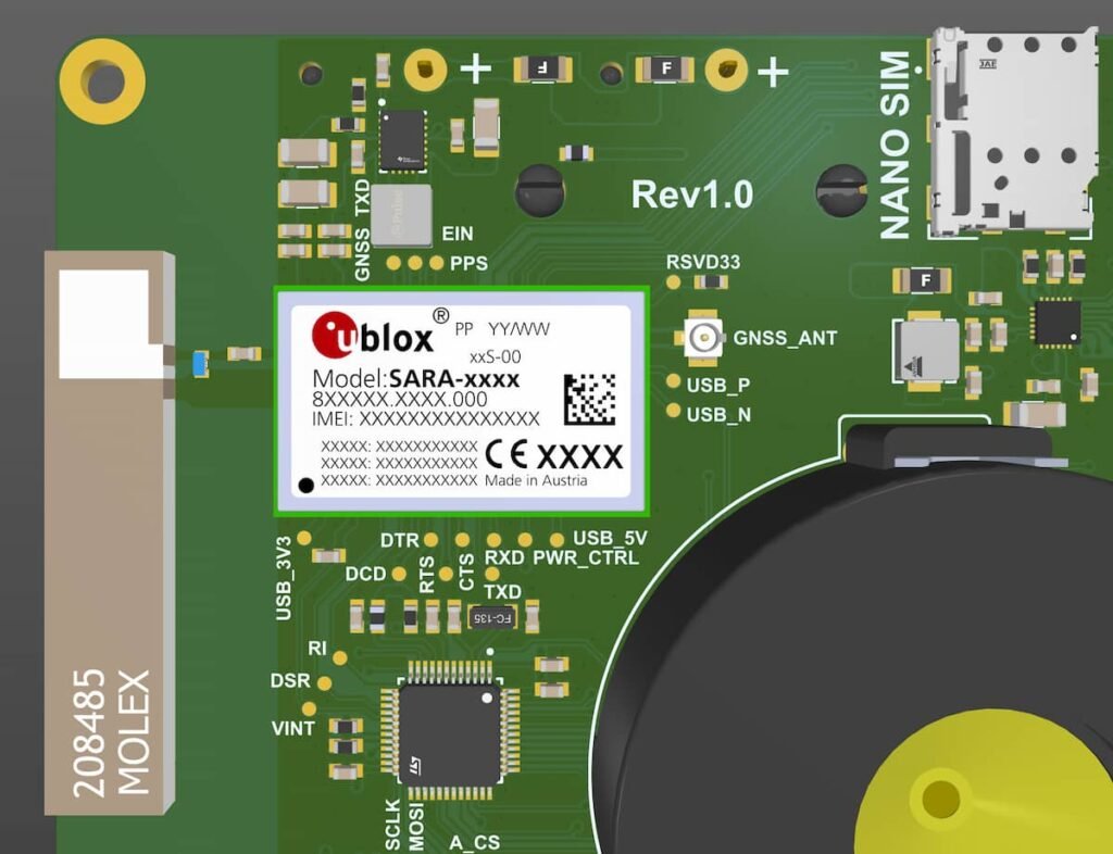
LTE module layout
The complexity of this project lies primarily in the layout and routing of the LTE module, which plays a vital role in the overall performance of the storage alarm PCB. Specifically, the RF networks and higher current nets, including the input power and LTE power, require careful attention to detail. With that in mind, let’s explore the intricate arrangement and routing of the individual components within our LTE module, understanding their significance in achieving optimal functionality for the board.
LTE Module placement
In this PCB design, it is important to optimize the placement of the LTE module to minimize the length of the RF line and ensure a closer path from the DC source for VCC. Furthermore, it is crucial to separate the module, analog parts, and RF circuits from potential sources of radiated energy. Digital circuits, in particular, have the potential to emit digital frequency harmonics, which can cause electro-magnetic interference and impact the performance of the module, analog parts, and RF circuits.
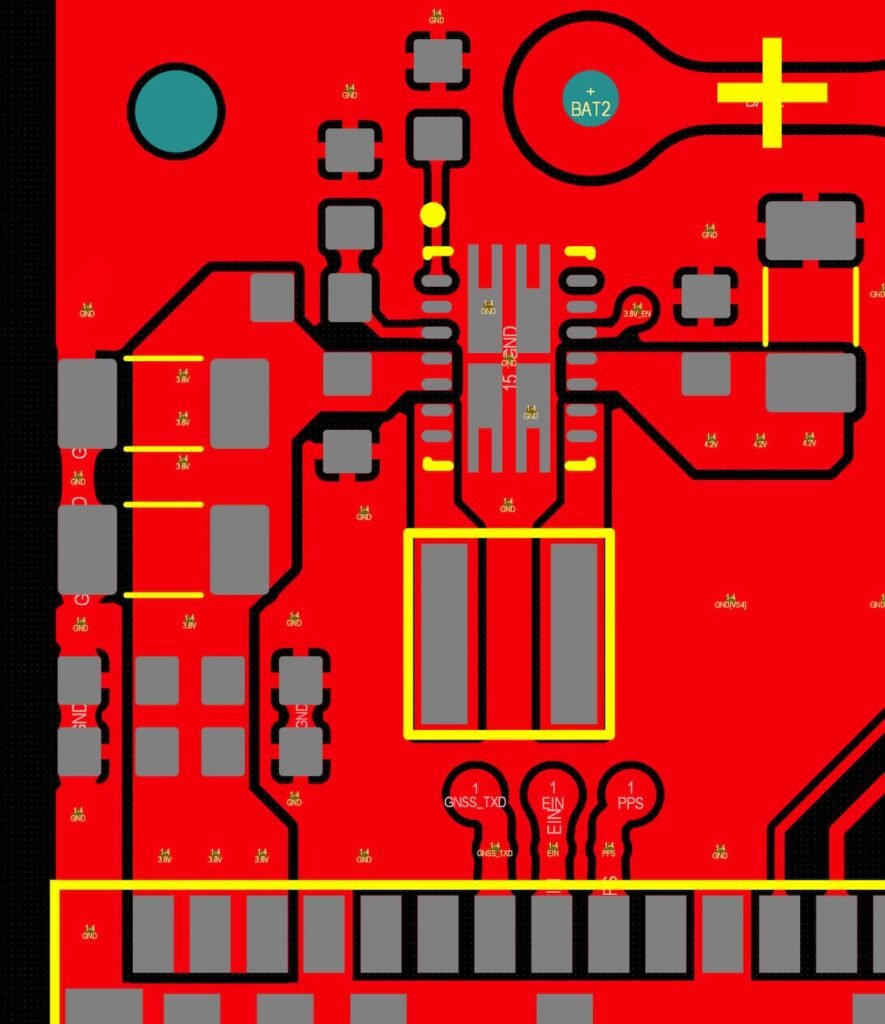
To ensure optimal performance, I positioned the module in a way that maximizes the distance between the antenna and the VCC supply line and its associated components (refer to Figure 5). This placement helps minimize any potential interference between these critical elements.
Additionally, it is crucial to consider the heat dissipation during continuous transmission at maximum power, as it can significantly raise the temperature of the PCB beneath the SARA-R4 series modules. Of course, the system as a whole must always be considered too. In this system, the LTE module will work quite rarely, it will usually be in sleep mode, so the PCB should not get very hot. However, I still recommend that you place temperature-sensitive components as far away from the LTE module as possible.
VCC layout design
To ensure optimal power routing for the LTE module in my storage alarm system project, it is crucial to adhere to specific guidelines outlined in the datasheet. If you are a bit lazy to read the datasheet, then in short, we need to focus on keeping the VCC track short and wide, and place bypass capacitors as close to the LTE module as possible.
To achieve correct RF performance, establishing a solid connection between the module’s VCC pins and the DC power supply is essential. In my design, I took care to connect the VCC to the power supply using a trace that is both wide and as short as possible. Moreover, I did my best to route the VCC trace as far as possible from the antenna, as illustrated in Figure 6.
To address potential current spikes and ensure stable operation, I positioned a large tank bypass capacitor near the DC-DC output. Additionally, I placed another large bypass capacitor near the module to further mitigate current fluctuations. It’s important to note that components with high equivalent series resistance (ESR) should be avoided.
Equally important is the placement of bypass capacitors in the picofarad (pF) range. In my case, I used a 47pF capacitor, which I positioned directly at the VCC pins where the VCC line narrows near the module’s VCC input pins. This enhances the rejection of RF noise within the frequency band centered around the Self-Resonant Frequency of the pF capacitors. This approach is highly recommended, especially when the application device incorporates an internal antenna.
Grounding layout design
The SARA-R4 LTE module comes with numerous ground pins, which is beneficial for reducing ground bounce by minimizing the inductance in the ground paths. It is crucial to establish a solid connection between the module’s GND pins and the application board’s ground layer to ensure optimal RF performance. This connection not only significantly reduces EMC issues but also acts as a thermal heat sink for the module.
As I discussed earlier, the PCB design involves multiple layers, including a dedicated solid ground plane. The VCC supply current returns to the main DC source through the ground as the ground current. Therefore, it is vital to create a suitable and uninterrupted ground plane that serves as an adequate return path to the main DC source. To achieve this, I strategically placed vias at each GND pad surrounding VCC pins. Additionally, I used via stitching to connect all the GND areas together, using a complete via stack that goes down to the main ground layer of the board.
Antena layout
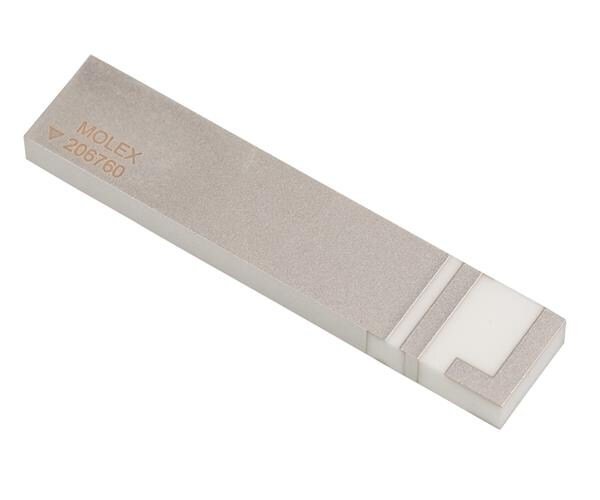
For my project, I opted to use an integrated surface-mount ceramic antenna (Figure 7). The placement of the antenna plays a crucial role, and it is essential to adhere to the manufacturer’s guidelines regarding its placement and routing.
Following the recommendations of the LTE module manufacturer, I positioned the antenna far away from the VCC supply line, related components, high-speed digital lines, and potential sources of noise. It is crucial to keep the antenna as far away as possible from sensitive circuits. Also, on a multilayer board, the whole layer stack below the RF connections should be free of digital lines.
The SARA-R4 series modules provide an RF interface for connecting an external antenna. The ANT pin serves as the RF input/output for transmitting and receiving RF signals. To ensure proper transmission and reception of RF signals, the ANT pin should be connected to the external antenna via a 50 ohm transmission line.
To minimize parasitic capacitance to ground, it is advisable to increase the clearance of GND around the ANT and ANT_GNSS pads on the top layer of the application PCB, ensuring a minimum distance of 250 μm up to the adjacent metal-defined pads. And that’s what I did, as shown in Figure 8.

When dealing with RF circuits, it is crucial to evaluate the performance and routing of the initial prototype using a network analyzer. This evaluation will help determine if any adjustments or tuning are necessary. While the manufacturer’s recommendations or a reference design’s routing can provide a starting point, they should be considered as initial guidance to help you approach an optimal design for your first prototype.
SIM layout
When designing the layout for the SIM card interface lines, certain issues may arise if the SIM card is either positioned far from the LTE module or located in close proximity to the RF antenna.
In the first scenario, having a long connection can lead to the radiation of some harmonics of the digital data frequency. To mitigate this problem, I made sure to keep the SIM traces as short as my mechanical design allowed me.
In the second case, these same harmonics can be picked up, resulting in self-interference that can negatively impact the sensitivity of LTE receiver channels operating at frequencies coinciding with the harmonics. To prevent this, I used RF bypass capacitors placed as close as possible to the SIM card connector. This helps in reducing self-interference and maintaining optimal channel sensitivity.
Furthermore, considering that the SIM card is typically handled by end users, there is a possibility of electrostatic discharge (ESD) discharges. To safeguard against this, I included TVS diodes, which I placed as close as possible to the pins of the SIM card connector.
Completing the Board
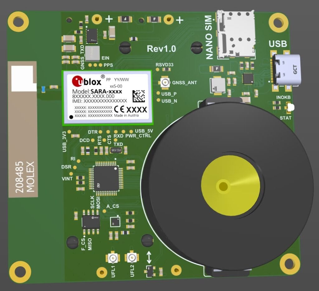
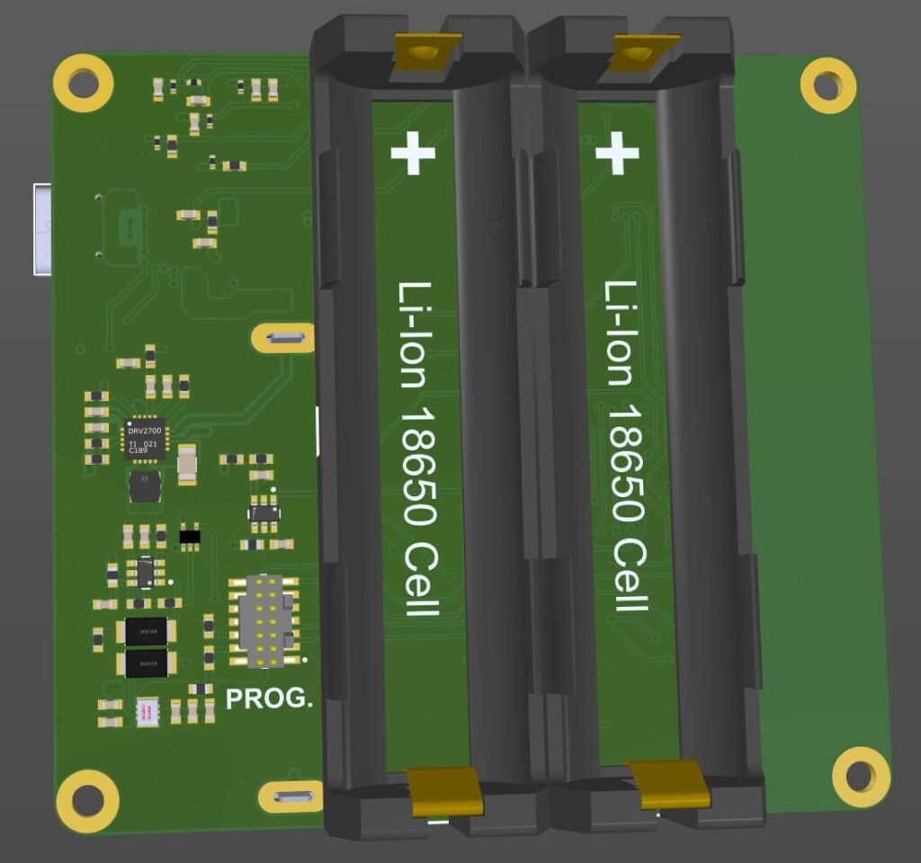
So after putting all the components together and connecting all the tracks, the board was complete. The 3D model of the completed board is shown in Figure 9 and Figure 10.
Board assembly
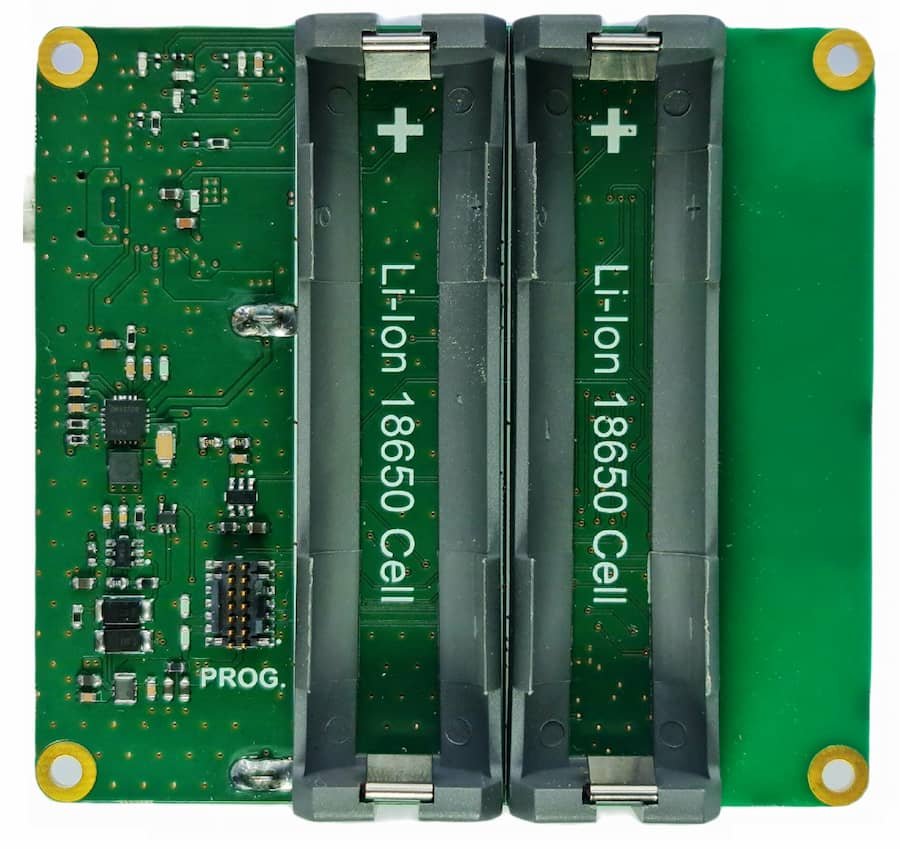
The process of soldering proved to be quite challenging, requiring more than just a soldering iron. In particular, the multitude of surface-mounted components with pads located under the IC necessitated the use of a hot air rework station. As I soldered all of the components one by one, I couldn’t help but feel a pang of regret for not ordering a stencil beforehand. With a stencil, I could have made the soldering process easier and faster. Nonetheless, I pressed on and finished the assembly of the board in one sitting. The assembled board is shown in Figure 11.

Summary
In the second part of this series on building a DIY alarm system circuit, I focus on designing the PCB. A well-designed PCB layout is crucial for optimal performance, signal integrity, and ease of assembly. I opted for a 4-layer PCB to accommodate the components and minimize noise interference. The layer stackup provided improved power and ground plane distribution, particularly important for RF components.
I discussed the layout considerations for specific components such as the piezo driver circuit, USB-C charger, magnetic sensor, accelerometer, LTE module, and SIM card. I highlighted the importance of factors like ground planes, thermal dissipation, component placement, trace routing, decoupling capacitors, and antenna placement.
Throughout the article, I provided visual references and figures to aid in understanding the layout and placement of the components. By following the guidelines and techniques outlined in this article, you’ll be able to design a PCB layout that ensures optimal functionality, signal integrity, and ease of assembly for your DIY alarm system.