A Molded Interconnect Device (MID), to put it simply, is an injection-molded plastic device that combines mechanical and electrical functionality. This plastic part incorporates a conductive material pattern similar to a printed circuit board (PCB). Usually, MIDs are the solution for routing interconnections, or mounting components, on a three-dimensional (3D) surface (Figure 1). Interconnections can be made along any surface of the 3D part.
Where are MIDs Used?
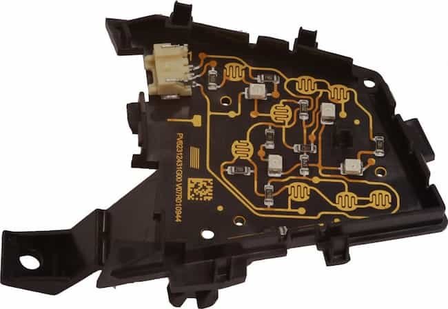
The adoption of Molded Interconnect Device is not very widespread. MIDs are found in all industries, but the key markets are telecommunication, medical, automotive and consumer electronics. Integrated antennas in mobile devices like tablets or phones are one example of a typical application for MIDs. The car’s steering wheel switch module could serve as another illustration (Figure 2). But to be completely honest, MID applications are still fairly uncommon and it is difficult to find usage examples, even on Google. How many distinct examples can you find if you try searching for MID application examples?

Advantages of MIDs
Regarding the advantages of MIDs, well, there ain’t that much. The selling points for MIDs are space saving, weight reduction, and part count reduction. An alternative to conventional PCBs, MIDs add electrical connectivity to the surface of 3D structures. Therefore, for now, it only makes sense to use MIDs where normal wire connections are not possible due to space limitations.
Disadvantages and limitations of MIDs
The main reason why MIDs have not become widely used is the circuit density of these devices. MIDs can have two conductive layers, top and bottom, while a PCB can have dozens of layers. Additionally, we must note that there are limitations on how components can be mounted on the 3D structure’s surface. Components on a PCB can be mounted on the top and bottom sides using a pick and place (PnP) machine. The top and bottom sides are assembled separately. It is not that simple with MIDs. Components can be mounted on any surface, which means standard PnP machines cannot be used.
How are MIDs Made?
Although there are numerous methods for producing MIDs, two-shot injection molding and laser direct structuring are usually used.
Two-Shot Molding
In two-shot injection molding, the circuit carrier is produced in two successive injection molding processes. Here, two distinct plastic materials are used. One of the two materials has a catalyst mixed into it so that the conductor paths can be selectively mapped during the metallization. Typically, a mechanically more stable part is produced first. This first injection forms the basis for the second shot.Following molding, the part undergoes a chemical pretreatment that increases surface roughness and helps copper adhere to the mold. Following this, copper traces are created on the plastic part using an electroless metallization process.
Laser DirectStructuring (LDS)
In laser direct structuring (LSD), parts are made using one-component injection molding. The part is made of plastic with special additives. The conductive pattern is then structured by the laser beam. Laser energy activates a special additive and forms a rough surface on which the copper can be firmly attached during metallization. The conductive tracks are then formed in an electroless copper bath. The metallization takes place only in the laser-structured areas of the plastic part. I highly advise visiting the LPKF website and viewing the video on the LDS process to get a better understanding of this procedure.
How are MIDs Designed?
In general, the methods used in MID technology are similar to those used in traditional plastics engineering. Therefore, you must first create a plastic part that will serve as a circuit carrier. For this, you need computer modeling software to create an object within a three-dimensional space. Software like Solidworks, Autocad, or equivalents, can be used.
Next, you will need software that allows you to design electronic schematics, lay traces, and component pads on the 3D part. For instance, 3D layout is supported by Altium Designer. It enables you to synchronize your library footprints and schematic documents with 3D circuit design.
To demonstrate how MIDs are designed, I made a simple circuit that allows me to light a led by pushing a button (Figure 3). Then I used Solidworks to create a simple circuit carrier.

Using Altium Designer, I imported the circuit carrier and synchronized components from the schematic to the 3D PCB Editor. Following component placement, I routed traces between component pads using Altium Designer’s 3D routing tools. Any surface of the 3D part can be used for routing and component placement (Figure 4).