The L6470 is a fully integrated motor driver. It provides a complete standalone solution for stepper motor applications. The L6470 is controlled by a host microcontroller (MCU) through a fast 8-bit serial peripheral interface (SPI). Multiple L6470 drivers can be connected in a daisy chain configuration. Most likely, if you are here, you have read the L6470 datasheet. Additionally, you may have noticed that there is not a lot of information available on how to pack data into an SPI frame when drivers are connected in a daisy chain configuration. This article describes the method for synchronous serial communication to multiple L6470 motor driver devices using SPI with daisy chain functionality.
Serial Peripheral Interface
SPI is a type of serial communication interface that allows synchronous data transfer between a microcontroller and one or more peripheral devices. Here we will talk about MCU and L6470 motor driver communication via SPI. Keep in mind that the L6470 is always a slave. MCU generates a clock signal (CK), a chip signal (CS), and a serial data out (SDO) signal. When CS is forced low, communication begins. The CK line is used for synchronization of data communication. All commands and data bytes are shifted into the device through the serial data input (SDI). Data is transmitted with the most significant bit (MSB) first. The SDI is sampled on the rising edges of the CK. All output data bytes are shifted out of the device through the SDO output. The SDO is latched on the falling edges of the CK. When a return value from the device is not available, an all zero byte is sent. After each byte transmission, the CS input must be raised and kept high for at least 800ns in order to allow the L6470 to decode the received command and put the return value into the SHIFT register.
L6470 Daisy Chain Electrical Connections
As previously stated, multiple L6470 drivers can be linked together in a daisy chain configuration. The L6470 is always a slave, and the MCU is a master. Figure 1 shows an example of the daisy chain configuration, which can be found on page 39 of the L6470 datasheet. We’ll use it to explain electrical connections between chips.
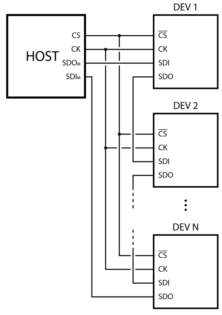
From Figure 1, we can see that the daisy-chain configuration for the L6470 is as follows:
- The MCU CS line is connected to the CS input of all the slaves.
- The MCU CK line is connected to the CK input of all the slaves.
- The SDI input of the first slave in the chain is connected to the MCU SDO.
- The SDO output of each slave is connected to the SDI input of the next slave, except for the last slave of the chain.
- The MCU SDI is connected to the SDO output of the chain’s last slave.
To save host GPIOs in a daisy chain configuration, BUSY pins of different slaves can be hard-wired and FLAG pins can be or-wired.
Keep in mind that increasing the number of devices connected in a daisy chain configuration may degrade SPI communication performance. The maximum number of devices that can be connected in a daisy-chain configuration depends on the clock skew.
The downside of daisy chains is that as the number of slaves grows, communication speed declines. This happens because every time a byte has to be transmitted to a device, the whole slave chain has to be filled. Despite this, it has some benefits. The daisy chain configuration allows perfect synchronization in the execution of the commands by the slave devices. This is due to the fact that when the CS line is raised high, all devices simultaneously acquire the respective transmitted byte.
L6470 SPI Daisy Chain Communication
In Daisy Chain configuration, all slaves act as a single slave. It can be thought of as a single unit that contains a number of bytes. Every time the master needs to receive or transmit a byte from or to a slave, it must fill all the shift registers of the slaves.
In a daisy chained system, the first slave receives data directly from the microcontroller. This data is clocked into the first slave’s internal shift register. As long as CS remains low, this data propagates through to the first slave’s SDO output. The SDO of the first slave goes into the SDI of the second slave, so the data is clocked into the second slave’s internal shift register as the data appears on the first slave’s SDO output. Just as the second slave receives its data from the first slave, the microcontroller can simultaneously send another command to the first slave. This new command overwrites the previous data in the first slave’s shift register. As long as CS remains low, the data propagates through the entire daisy chain until each of the slave devices has received its appropriate command. The command loaded into each slave’s shift register executes on the rising edge of CS.
So the first byte transmitted by the master is received by the last slave in the chain. And the last transmitted byte is received by the first slave in the chain.
The response bytes from the slave chain are addressed similarly. The first byte received by the master is transmitted by the last slave in the chain. And the last received byte is transmitted by the first slave of the chain.
L6470 SPI Daisy Chain Examples
In the following section, we’ll analyze a communication example with two L6470 motor drivers that are connected in daisy chain configuration. Here we will use the X-NUCLEO-IHM02A1 two axis stepper motor driver expansion board (figure 2). This board is based on the L6470. The SPI peripheral of each L6470 is connected in a daisy chain configuration.
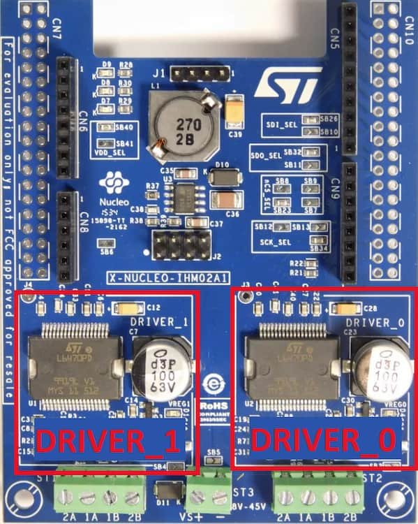
We can see from the X-NUCLEO-IHM02A1 expansion board’s schematic that DRIVER 1 is the first slave in the chain and DRIVER 0 is the second (or last). This means that DRIVER 0 receives the first byte sent by the microcontroller, and DRIVER 1 receives the second byte.
For SPI daisy chain communication examples, we will not configure the motor driver, and we will leave all registers and flags with their default values. The RUN command will be used to analyze SPI data flows. This command structure is shown in Figure 3.
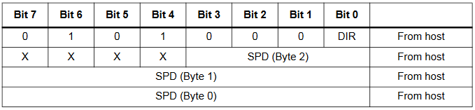
The Run command is constructed from four bytes. This command produces a motion at SPD speed; the direction is selected by the DIR bit: ‘1’ forward or ‘0’ reverse. Using a logic analyzer, let’s analyze three scenarios:
- Run DRIVER_0 in the forward direction at 500 step/s.
- Run DRIVER_1 in the forward direction at 500 step/s.
- Run both DRIVER_0 and DRIVER_1 at the same time. The DRIVER_0 will be set to move at a rate of 500 steps/s. And the DRIVER_1 will be programmed to run backwards at a rate of 250 steps/s.
RUN DRIVER_0 example
Since we want to run DRIVER_0 in the forward direction, we need to set the DIR bit (DIR=’1’). So the first byte that we need to send from MCU must be 01010001 in binary or 51 in hexadecimal. The last three bytes of the Run command hold the speed (SPD) value. This value sets the speed for stepper motors. The SPD value is expressed in step/tick. In order to convert steps per second to SPD, the following formula can be used:
$$SPD = \frac{[steps/s] \cdot 250ns}{2^{-28}}$$
From the above equation, we can calculate that for 500 steps/s, we must transfer a value of 33554 with the last three bytes. The calculated value needs to be converted into three bytes. This can be achieved by doing this:
ByteToSend[1] = (uint8_t)(value >> 16);
ByteToSend[2] = (uint8_t)(value >> 8);
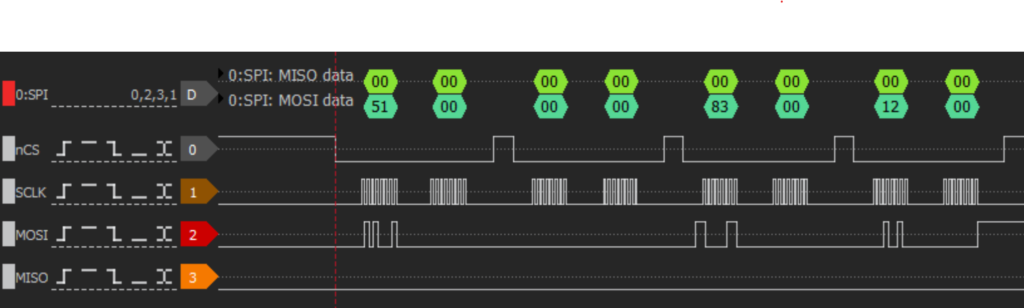
ByteToSend[3] = (uint8_t)(value);From the information above, we can see that for the DRIVER_0, we need to transfer these four bytes: 0x51, 0x00, 0x83, and 0x12 (these numbers are in hexadecimal). The Nop command, informing the driver to take no action, should be sent to DRIVER_1. For the L6470, the Nop command is all zeros (0x00).
The complete data transfer sequence from the MCU to drivers should look like this:
- CS pulled low. The MCU transmits two bytes: 0x51 and 0x00. CS pulled high.
- CS pulled low. The MCU transmits two bytes: 0x00 and 0x00. CS pulled high.
- CS pulled low. The MCU transmits two bytes: 0x83 and 0x00. CS pulled high.
- CS pulled low. The MCU transmits two bytes: 0x12 and 0x00. CS pulled high.
To illustrate the data transfer sequence, we hooked up a logic analyzer to the SPI pins of the MCU. The result that we got from the logic analyzer is shown in Figure 4. As you can see from this image, the SPI communication line marking is different from what we used before. This is due to the fact that devices other than MCUs with SPI interfaces typically use the SDI/SDO or DIN/DOUT convention. But MCUs always use the Master In Slave Out (MISO) and Master Out Slave In (MOSI) convention. Since we are capturing data from the MCU, we are using the MOSI/MISO convention to name the SPI lines.
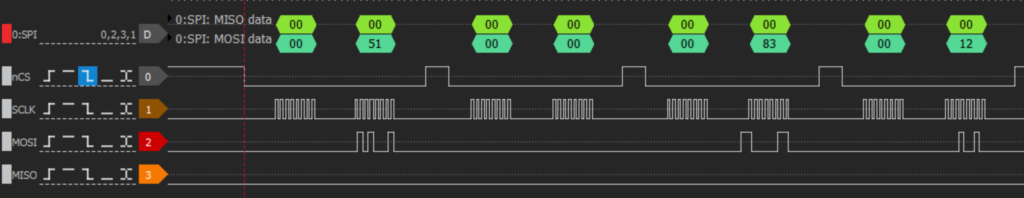
RUN DRIVER_1 example
This example is similar to the first one. The only difference is that the L6470 motor driver position in the SPI chain is different. As we previously discussed, DRIVER_1 is the first slave in the chain. Therefore, in this case, the last byte must be clocked into the DRIVER_1 internal shift register. The DRIVER_0 must receive the Nop command, which in this example is the first byte.
The complete data transfer sequence from the MCU to drivers should look like this:
- CS pulled low. The MCU transmits two bytes: 0x00 and 0x51. CS pulled high.
- CS pulled low. The MCU transmits two bytes: 0x00 and 0x00. CS pulled high.
- CS pulled low. The MCU transmits two bytes: 0x00 and 0x83. CS pulled high.
- CS pulled low. The MCU transmits two bytes: 0x00 and 0x12. CS pulled high.
The data transfer sequence captured by the logic analyzer is shown in Figure 5.
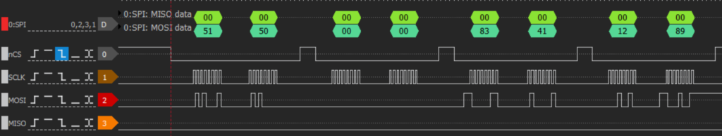
RUN both DRIVER_0 and DRIVER_1 example
This time, we will run both motors at the same time. Command execution by the slave devices will be synchronized. Here, DRIVER_0 will get the command to run in the forward direction at 500 steps/s. The DRIVER_1 will get the command to run in the reverse direction (0x50) at 250 steps/s (0x00, 0x41, 0x89).
The complete data transfer sequence from the MCU to drivers should look like this:
- CS pulled low. The MCU transmits two bytes: 0x51 and 0x50. CS pulled high.
- CS pulled low. The MCU transmits two bytes: 0x00 and 0x00. CS pulled high.
- CS pulled low. The MCU transmits two bytes: 0x83 and 0x41. CS pulled high.
- CS pulled low. The MCU transmits two bytes: 0x12 and 0x89. CS pulled high.
Figure 6 shows the data transfer sequence for both motor drivers that was captured by the logic analyzer.