A buck converter is a simple type of DC-to-DC converter that produces an output voltage that is less than its input voltage. In other words, this DC-to-DC converter steps down the voltage from its input to its output. Hence, it is also called a step-down converter. Typically, a high-side transistor switch is used in the basic buck converter, but a low-side switch can be used too. In this article, we will discuss the difference between low-side and high-side switching. We’ll also analyze the low-side buck converter circuit.
Fun fact: The buck converter’s name derives from the fact that the inductor always “bucks” or operates in opposition to the input voltage.
Low-side vs. high-side switch in a buck converter
Typically, a high side transistor switch is used in a basic buck converter. We’ll concentrate on the MOSFET in this instance. As a high-side switch, a MOSFET with either P- or N-channels may be used. Both the gate capacitance and the drain-source on resistance of the P-channel MOSFET are greater than those of the N-channel MOSFET. Thus, the N-channel MOSFET is preferred for applications requiring larger current. To control the N-channel MOSFET on the high side, a floating gate driver circuit is required. This circuit is both pricey and somewhat complex. Therefore, for some applications, a low-side switch is preferred.
The advantage of the low-side switch is a simpler control circuit. Here, the N-Channel MOSFET source is connected to the ground. To allow current to flow through the channel, the N-channel MOSFET gate terminal must be made more positive than the source. This means that a complex control circuit is not necessary. The MOSFET can be driven by a microcontroller. The downside is that the load is not ground-referenced. When the MOSFET is turned on, there is still a small voltage drop across it. Because of that voltage drop, the ground for the switched-on device is not at 0 volts.
When to use a low-side switch
A good rule of thumb is that if you are supplying power to an entire circuit, then a high-side switch should be used. However, if you are turning a device on and off, a low-side switch is an easy, low-cost, and effective solution.
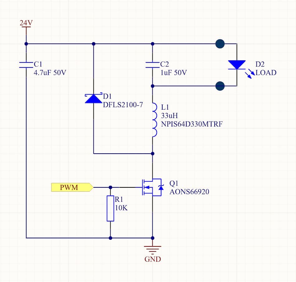
Basic circuit diagram of a low-side buck converter
Figure 1 depicts an example of a low-side buck converter circuit.
How a low-side buck converter works
Similar to many other power supply topologies, the buck converter works on the principle of storing energy in an inductor. The inductor stores energy in the form of a magnetic field. The voltage drop across an inductor is proportional to the change in electric current flowing through it. The inductor tries to oppose the current by producing a voltage to counteract this change. An ideal buck converter’s output voltage is equal to the product of the switching duty cycle and the supply voltage.
To simplify the explanation, we will assume that the converter is made of ideal components. In this case, there is no voltage drop across the MOSFET or diode. Moreover, no current flows through them when they are turned off. The inductor has zero series resistance.
The buck converter operation can be broken down into two states: when the MOSFET is turned on and when it is turned off. If I try to explain the operation of this circuit in a lengthy text, it will be hard to follow. Therefore, I will divide these two states into smaller steps.
State 1: The MOSFET is turned on.
- At the beginning, when the MOSFET Q1 is turned off, no current is flowing in the circuit.
- When the MOSFET is turned on, the current will begin to flow through the load D2 and the inductor L1.
- As the current through the inductor increases, the magnetic field in that inductor will also increase.
- The inrush of current creates a potential across the inductor that opposes the supply voltage.
- This voltage drop through the inductor reduces the net voltage across the load.
- Over time, the rate of change of current decreases, and the voltage across the inductor also decreases, increasing the voltage at the load. During this time, the inductor stores energy in the form of a magnetic field.
- Energy is stored in both the inductor L1 and the capacitor C2.
- In this stage, the flyback diode D1 is reverse-biased and does not conduct.
Stage 2: the MOSFET is turned off.
- If the MOSFET Q1 is turned off while the current is still changing, then there will always be a voltage drop across the inductor. That means the net voltage at the load will always be less than the input voltage.
- When the MOSFET is turned off, the energy stored in the magnetic field around inductor L1 is released back into the circuit.
- The voltage across the inductor is now of the opposite polarity from the voltage generated when the current was increasing.
- Now the flyback diode D2 is forward biased, and it provides a return path for the inductor current.
- The stored energy in the inductor’s magnetic field powers the load through the diode with a decreasing current. During this phase of the switching cycle, the inductor becomes the primary source of output power.
- As the inductor continues to deliver its stored energy to the load, the inductor current will begin to drop. This current decline lasts until the next on-state, at which point the current rises to its prior value.
How a buck converter increases current.
As explained previously, even in the absence of current being drawn from the source (the MOSFET is turned off), current is still delivered to the load. The average current flowing through the load is therefore greater than the average current being drawn from the source.
A buck converter can output almost all the power it gets from its input. Usually, its efficiency is greater than 85 percent. This means that if the output voltage is significantly lower than the input, the output current can be significantly higher.