Consumers prefer smaller electronic devices. To make smaller devices, you need smaller electronic components. Due to the fine pad pitch of the components, standard via routing might not always be an option. In this case, a via in pad (VIP) is used. The design method known as “via in pad” involves placing the via directly on the copper pad of a surface-mounted component (SMD). In this article, we will cover the benefits of using a via in pad, when to use one, and how to design a printed circuit board (PCB) for it.
What is via in pad
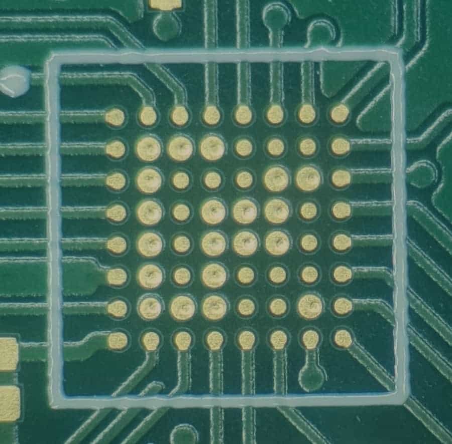
A signal is typically routed away from the pad before a via is placed. (Figure 1). This allows application of a solder mask on a trace connecting a via to a pad. During the soldering process, a solder mask prevents solder paste from wicking into the barrel of the via.
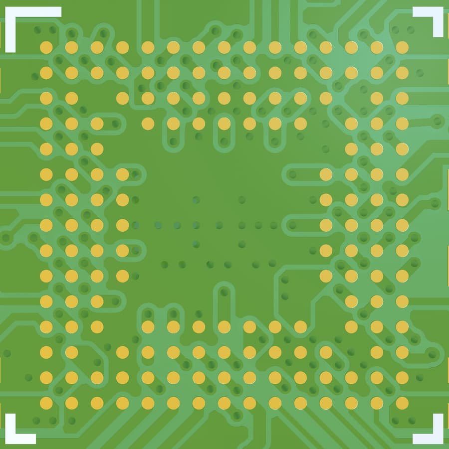
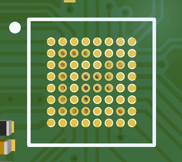
When a via is inserted into a component footprint pad, this is referred to as using a via in pad (Figure 2). In this case, the via is in the pad and there is no way to prevent solder paste from wicking into the barrel of the via. A completely filled via structure is required to avoid air entrapment and outgassing during assembly. Moreover, the via must be capped with conductive material so the component can be reliably soldered. This is accomplished by first filling the via with epoxy and then plating it over with copper.
When should the via in pad be used
A small component package size is the primary reason behind the use of via in pad technology. A via in pad is typically used with a BGA. For component packages with a sub 0.5mm pad pitch, it is practically impossible to fan out all connections using conventional routing methods. For a 0.5mm pad pitch component, clearance between pads is somewhere around 0.2mm. Since the majority of PCB manufacturers are unable to make traces and clearances smaller than 3 mil (0.076mm), 0.2mm is insufficient for even a single trace. The only feasible routing method for these small pitch components is via in pad routing.
Other advantages of via in pad (VIP) routing
- Via in pad is useful in high-speed designs because it reduces trace length and, as a result, inductance. It is very useful for high frequency component grounding. High frequency component grounding can benefit greatly from it.
- By eliminating surface routing, it is possible to place bypass capacitors close to the components’ power supply pins. For AC noise signals, this provides a low impedance path to ground.
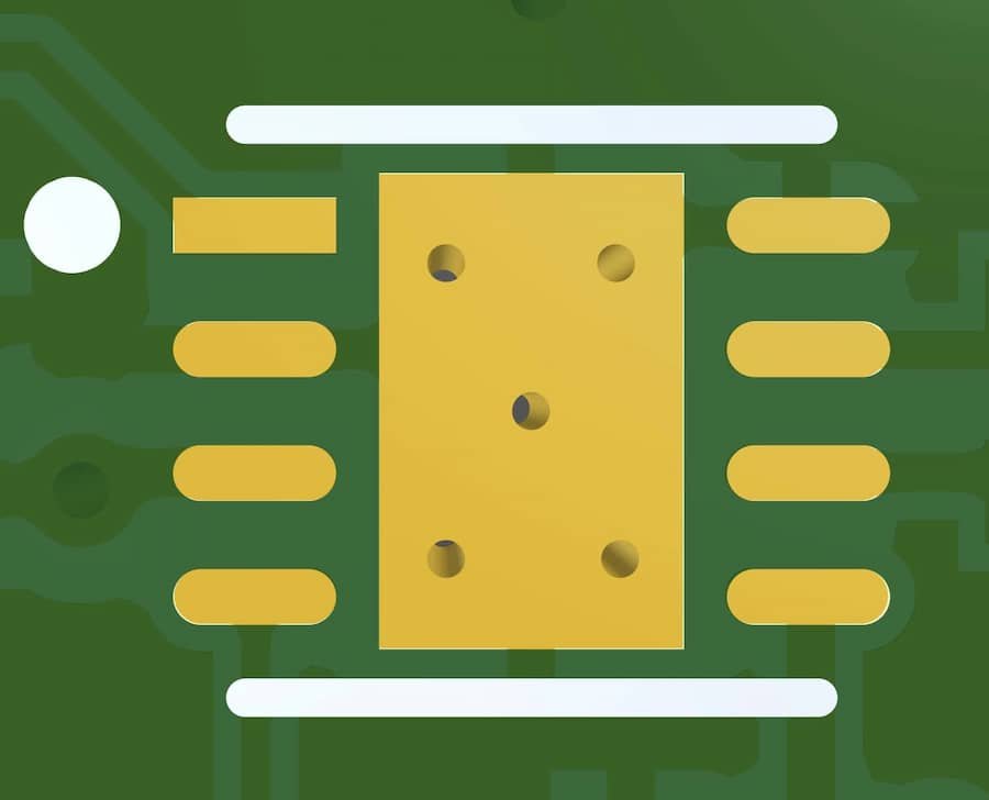
- Vias in pad without plugging and capping can improve thermal dissipation. Some components have a thermal pad that mounts to the PCB. The placement of a via in a thermal pad (Figure 3) causes any excess solder paste under the part to be pulled through the via. Extra solder paste that fills the vias improves the thermal conductivity of the via.
Disadvantages of via in pad (VIP) routing
The only true disadvantage of via in pad design, from the perspective of a PCB designer, is cost. For this kind of routing, the PCB manufacturers will have to fill and plate with conductive material vias, which will add new steps to the fabrication process. More steps means that producing the PCB takes more time. As more time and effort are required, the cost of the PCB increases.
PCB design for Via in Pad
From a design point of view, implementing via in pad is very similar to traditional vias. The only difference is that an additional manufacturing file is required, which just contains the vias in component pads that need to be filled and capped. Sometimes it is just enough to tell the PCB manufacturer what vias you want to be via in pad.
Keep in mind that an important factor is pad diameter. The minimum annular ring requirement of IPC Class 2 or Class 3 must be met when selecting a via size. The pad size of the via must be large enough to accommodate manufacturing tolerances.
