A buck converter is a type of DC-to-DC converter that is used to step down voltage from its input to its output. It is often referred to as a step-down converter. This converter is widely used in electronic devices. It is so popular because of its simplicity, high efficiency, and low cost. A buck converter performs conversion using a transistor switch and an inductor. Typically, a high-side transistor switch is used, but in the previous article, we explained how and why a low-side switch might be used too. In this article, we will analyze the basic buck converter circuit and explain its working principle.
Operating Principle of a Buck Converter
A buck converter works by using a switching element and an inductor. The switching element is used to control the flow of current through the inductor. The inductor stores energy in the form of a magnetic field. When a current is applied to the inductor, the amount of voltage drop across it is determined by the inductance value and the rate of change of current. The inductor tries to oppose the current by producing a voltage that is opposite of the input voltage. The output voltage of an ideal buck converter that works in continuous current mode (CCM) is determined by the duty cycle of the switching element and the input voltage:
V_{out}\approx V_{in}\cdot (duty\: cycle)
The switching element is controlled by pulse-width modulation (PWM). It is a method of controlling the amount of power delivered to a circuit by adjusting the pulse width of a digital signal. The duty cycle of the pulses defines the amount of power provided, while the frequency of the pulses determines the speed of the control. The power sent to the circuit can be changed by varying the frequency and duty cycle of the PWM signal.
We’ll examine the schematic for a buck converter in Figure 1. It is a basic buck or step-down converter circuit that you will come across quite often. Here, a MOSFET is used as a switching element. To make it simpler to grasp, we’ll divide the buck converter’s operation into two states: when the switching element (MOSFET) is turned on, and when it is turned off. Furthermore, we’ll assume that the converter is made of ideal parts.
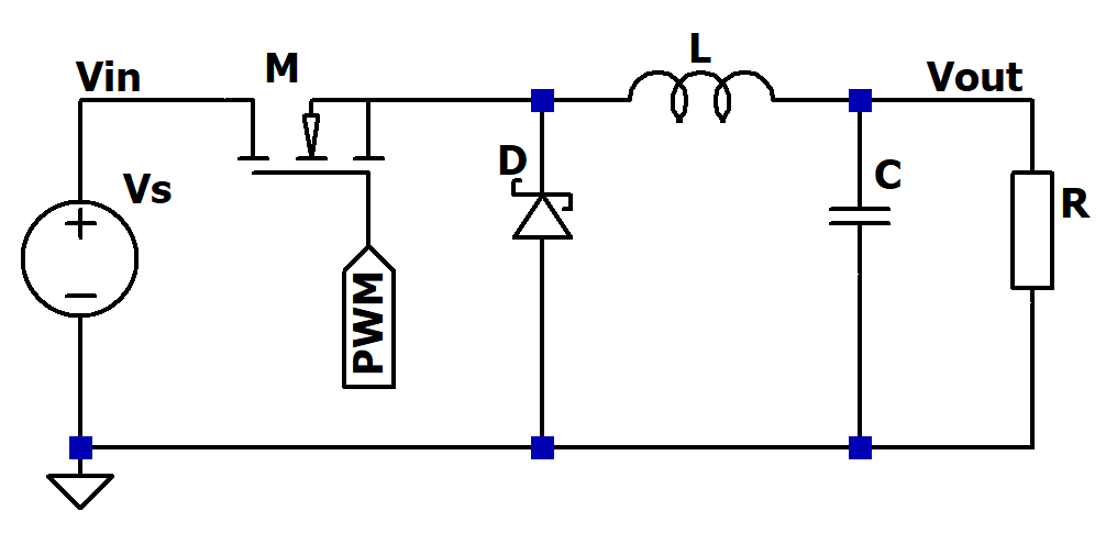
State 1: The switch is turned on
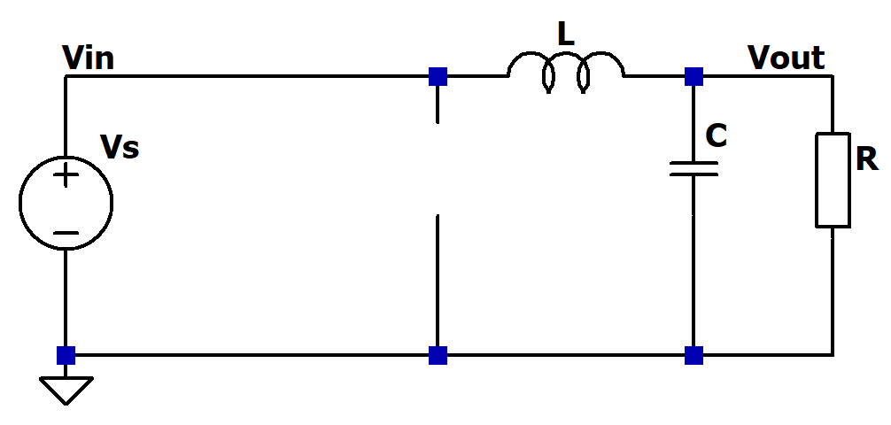
In this state, the MOSFET (M) is turned on and the diode (D) is reverse biased; therefore, we get the circuit shown in Figure 2. Let’s break down this state where the MOSFET is turned on into smaller steps. In doing so, we will be able to analyze this state more clearly.
1. At the beginning, when the MOSFET is turned off, no current is flowing in the circuit.
2. When the MOSFET is turned on, the current will begin to flow through the inductor (L), charging it up. The inductor current ramps linearly upward and is described as:
i_{L(on)}= \frac{(V_{in}-V_{out})\cdot t_{on}}{L}+i_{init}
As the current through the inductor increases, the magnetic field in that inductor will also increase. The inrush of current creates a potential across the inductor that opposes the supply voltage.
3. This voltage drop through the inductor reduces the net voltage across the load (R).
4. Over time, the rate of change of current decreases, and the voltage across the inductor also decreases, increasing the voltage at the load. During this time, the inductor stores energy in the form of a magnetic field.
5. Energy is stored in both the inductor and the output capacitor (C). The energy stored within the inductor during this period is:
E=(\frac{1}{2})\cdot L\cdot (i_{pk}-i_{min})^{2}
6. In this stage, the flyback diode is reverse-biased and does not conduct.
Stage 2: the switch is turned off
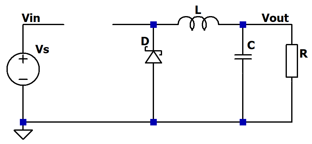
In this state, the MOSFET (M) is turned off, and now the diode (D) is forward biased; therefore, we get the circuit shown in Figure 3. Let’s break down this state into smaller steps as we did with the prior one and examine the circuit.
1. If the MOSFET is turned off while the current is still changing, then there will always be a voltage drop across the inductor. That means the net voltage at the load (R) will always be less than the input voltage.
2. When the MOSFET is turned off, the energy stored in the magnetic field around the inductor (L) is released back into the circuit.
3. The voltage across the inductor is now of the opposite polarity from the voltage generated when the current was increasing.
4. Now the flyback diode (D) is forward biased, and it provides a return path for the inductor current.
5. The stored energy in the inductor’s magnetic field powers the load through the diode with a decreasing current. During this phase of the switching cycle, the inductor becomes the primary source of output power.
6. As the inductor continues to deliver its stored energy to the load, the inductor current will begin to drop. The current through the inductor during this period is described as:
i_{L(off))}= i_{pk}-\frac{V_{out}\cdot t_{off}}{L}
This current decline lasts until the next on-state, at which point the current rises to its prior value.
Waveforms of a buck converter
The voltage waveforms of a buck converter can be divided into three main components: the input voltage, the switching voltage, and the output voltage.
- Input voltage: The input voltage is the DC voltage that is being converted by the buck converter. It is a higher voltage than the desired output voltage.
- Switching voltage: The switch voltage is the voltage at the inductor after a high-side switch. The switching voltage changes from zero to the input voltage when the switch is turned on and from the input voltage to zero when the switch is turned off. PWM is used to regulate this voltage change.
- Output voltage: The output voltage is the regulated DC voltage that is produced by the buck converter. This voltage in CCM is calculated by multiplying the input voltage by the high-side switch’s duty cycle.
The current through the inductor in a buck converter changes direction during each switching cycle as the high-side switch is switched on and off. The diode and voltage source also play important roles in shaping the current waveform. The current waveforms can be divided into three main components: the inductor current, the diode current, and the voltage source current. The waveforms shown in Figure 4 will be used to analyze these currents. The switching voltage is represented by the (a) waveform. It is a PWM waveform with a duty cycle of 50%. This means that the switch is turned on for 50% of the total period. Let’s look at the other three waveforms now.
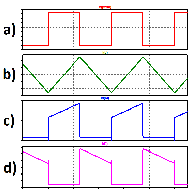
- Inductor current: Inductor current: The inductor current waveform (Figure 4. b) is divided into two different phases: charging and discharge. When the switch is turned on during the charging phase, the inductor current increases linearly (unless the inductor saturates). When the switch is switched off during the discharge phase, the inductor current decreases linearly.
- Voltage source current: When the switch is switched on, the voltage source delivers current to charge the inductor. The shape of the voltage source current waveform during the inductor charging phase is similar to that of the inductor current waveform (Figure 4. c).
- Diode current: When the switch is switched off, the inductor current continues to flow into the diode to charge the output. As a result, the current flowing through the diode during the inductor discharge phase is nearly identical to the current flowing through the inductor (Figure 4. d). The diode current decreases as the inductor current decreases.
The waveforms of a buck converter are complex and depend on many factors, such as the input voltage, the output voltage, the switching frequency, and the inductor and capacitor values.
How a buck converter regulates voltage
The buck converter output voltage is regulated by adjusting the duty cycle of the switching element. The duty cycle is the ratio of the time the switching element is turned on to the total period of the switching. The switching frequency is usually in the tens of kilohertz to a few megahertz range.
A feedback loop is often used to control the duty cycle of the switching element to maintain a constant output voltage. This feedback loop compares the output voltage to a reference voltage and adjusts the duty cycle as necessary to achieve the desired output voltage.
How a buck converter increases current
As explained previously, current is continually delivered to the load even after the switching element is switched off. As a result, the average current flowing through the load is larger than the average current taken from the source.
A buck converter can output almost all the power it gets from its input. Its efficiency is often better than 85%. This means that if the output voltage is much lower than the input voltage, the output current can be much larger.
Application of a buck converter
Buck converters are an important component in many electronic devices. They provide a lower, regulated DC voltage from a higher voltage source. These DC-to-DC converters have become popular in a variety of industries due to their high efficiency, compact size, and ability to handle high power levels. They are frequently found in consumer electronics, such as laptops and smartphones. They are also widely used in automotive electronics, industrial systems, renewable energy systems, telecom systems, medical devices, and military and aerospace systems.
Summary
In conclusion, the buck converter uses a switching element and an inductor to convert a higher DC voltage to a lower DC voltage. The switching element controls the flow of current through the inductor, and the inductor stores energy. The output voltage is regulated by adjusting the duty cycle of the switching element, which is controlled by a feedback loop to maintain a constant output voltage.